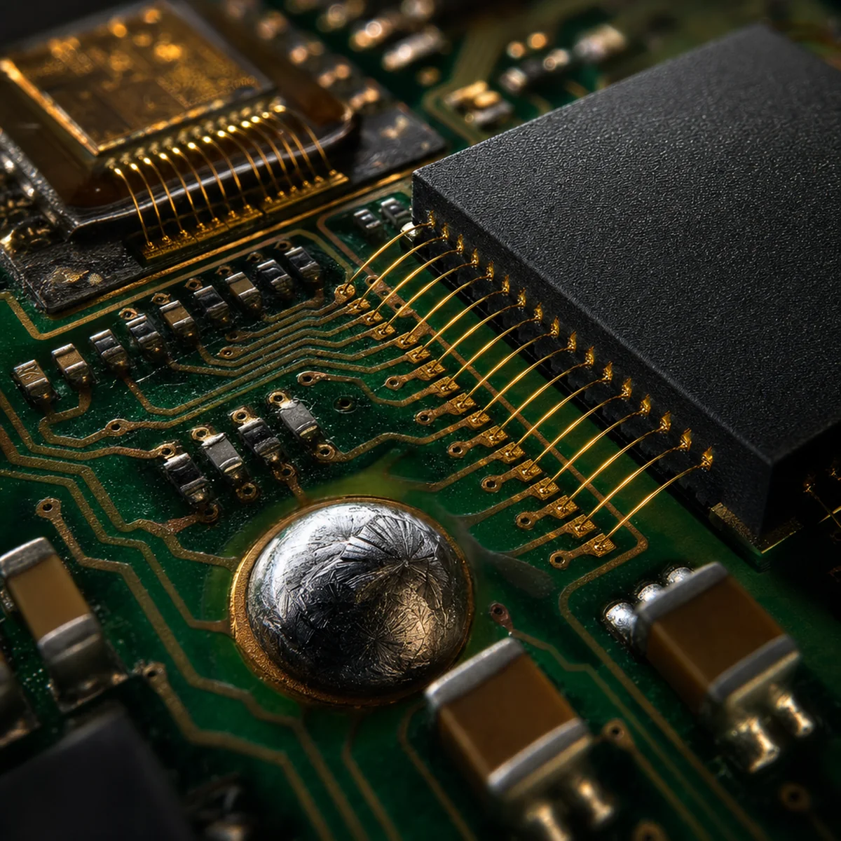
A wide 16:9 extreme macro photograph of a modern smartphone circuit board at 15:1 magnification, the microscopic components filling the frame as an alien city. Microchip packages rise like glass and black buildings from the green PCB substrate, their surfaces covered in microscopic bond wires — hair-thin gold wires arcing between chip pads and circuit board contacts, each one a perfect parabolic curve. The circuit traces running across the PCB are visible as copper highways, their surfaces showing the crystalline grain structure of the metal under the solder mask. Tiny ceramic capacitors and resistors sit in perfect rows like city blocks. A single solder joint is visible in macro detail — a perfect convex dome of tin-silver alloy with its crystalline surface structure revealed by the raking light. Single oblique fiber optic light from the left at 10 degrees. Color grade: deep green PCB, copper trace gold, black chip packages, the gold bond wires as the most brilliant elements. Mood: the hidden city inside every device, human ingenuity at its most miniaturized.